Buy PCB's Kits and Components for Audio Amplifiers Pre Amps BT boards Power supplies solar charge controllers Vu Meters & electronics parts at best price
- (+91) 9424930058
- mypcbinfo@gmail.com
- Amphead Electro Works, Aashish Complex, Ward No. 03 NH-46, Itarsi, Itarsi, Madhya Pradesh, India. 461111
© 2020 MYPCB. All Rights Reserved

400 Watts of Pure Sound - No Distortion, No Noise
This High power amplifier is liked by amateurs as well as professionals.
We revised the pcb 4 times so far based on customer feedback and our own testing.
Smaller in size and with metal tab connectors to support high currents.
New version PCB having space for Fitting Heatsinks Easily.
Features of 400 watt Hi-fi Amplifier Board
- High Power - 400 watt Dynamic output power .
- Very Low Distortion - 0.01% Total Harmonic Distortion at 120 watt output 1KHz sine wave .
- Speaker usability - 4 & 8 ohms, 100 watt to 600 watt Speakers can be used.
- Supply voltage - ±18 volts to ±45 volts DC supply working range.
- Protection - Fuses on each supply rail for preventing burnout due to fault or short circuit.
- Standard Components - All components used are available online or at your local electronics store.
- No SMD components used - only through hole components used, making soldering and replacement hassle free.
- Low cost - This amplifier can be made in a fraction of cost compared to similar amplifiers available in market.
Bengal Tiger Hifi Amplifier to make own -
- Musical instrument amplifier - Frequency response 20 Hz to 50 KHz, you can amplify any instrument like Guitar, Keyboard, Banjo.
- Amplified speaker box - Compact size board that can be fitted inside the speaker enclosure.
- Subwoofer Amplifier - High power amplification of low frequency sound.
- PA System - Public address system sufficiently audible at medium distance or over small area like family functions, Puja or Wedding Parties.
- Stereo Amplifier - Listen to your favorite songs in clarity never experienced before.
Brief description of 400 watt Hi-fi Amplifier Circuit :-
Input Stage
Input stage works as a transconductance amplifier ( voltage in - current out ).
This stage consist of Long Tailed Pair (LTP) made of Q1 & Q5, working as differential amplifier.
Input signal received at the base of Q1 is amplified and sent to VAS from collector. Negative feedback (NFB) received at the base of Q5 from output determines overall gain and balance of the amplifier.
Constant current is supplied to the LTP by Constant Current Source (CCS) made of Q2.
Collector currents of LTP transistors is balanced by Current Mirror (CM) made of Q3 & Q4.
In simple words input signal is amplified by the input pair Q1 & Q5 and sent to VAS for further amplification.
Voltage Amplification Stage (VAS)
As the name suggests, all the voltage gain of the amplifier is achieved in VA Stage.
The VA stage is Darlington (Beta Enhanced) which has better performance then single transistor VA stage.
Signal received from input stage at the base of Q6 is amplified via Darlington pair Q6 & Q9. Voltage amplified signal sent to the base of driver transistor Q11 from the Collector of Q9.
Constant current is supplied to VAS from CCS made of transistor Q7.
Biasing circuit is made of transistor Q8, which works as voltage divider. With preset RV1, base current of output transistors can be precisely adjusted.
Important to note that the biasing transistor Q8 must be fitted on the same heatsink along with output transistors to ensure thermal tracking and feedback.
In simple words signal received from input stage is amplified by Q6 & Q9. voltage amplified signal is sent to output stage.
Output Stage ( OPS )
This circuit has Class AB output stage, so each half of the signal is amplified by each pair of NPN and PNP output transistors.
Driver Transistors Q10 & Q11 work as buffers to prevent excessive loading of VAS and also provide input to the output transistor pairs of Q12, Q14 and Q13, Q15 respectively.
Emitter follower topology is used for output transistors which ensures minimum Crossover distortion.
Thermal feedback via transistor Q8 is necessary to prevent output transistors from destruction by thermal runaway.
Zobel Network - made of R30 & C10, provides protection against high frequency oscillations.
Inductor L1 is used to reduce harm from Capacitive load of Speakers Cables.
In simple words signal received from VAS is given to the output transistors via driver transistors. Output transistors conduct high current to drive the speakers load.
Amplifier Type & configuration
- 3 Stage Class AB amplifier
- INPUT - Long tailed pair with Constant current source and current mirror.
- VAS - Darlington VAS with biasing control preset, biasing transistor mount on main heatsink.
- OPS - Emitter follower NPN - PNP driver and power output transistor pairs.
Input and Gain
- Input Signal Sensitivity - 200mV to 1.5V ( Peak to Peak) 3V AC for Max power
- Gain - 26.8 dB ( Default )
- · Frequency Response ( 20Hz - 20Khz ) - ±0.5 dB
- Noise at Output - 110 nV/Hz1/2
Maximum Dynamic Power Output :-
Output power at various supply voltages -
- ± 18v = 50 Watt
- ± 24v = 100 Watt
- ± 35v = 200 Watt ( Recommended )
- ± 45v = 400 Watt ( High Heat )
Standard Test configuration for output power measurement -
- 2SC5200 2SA1943 Power transistors.
- 1Khz Sine wave input signal.
- 4Ω 800 watt load resistors
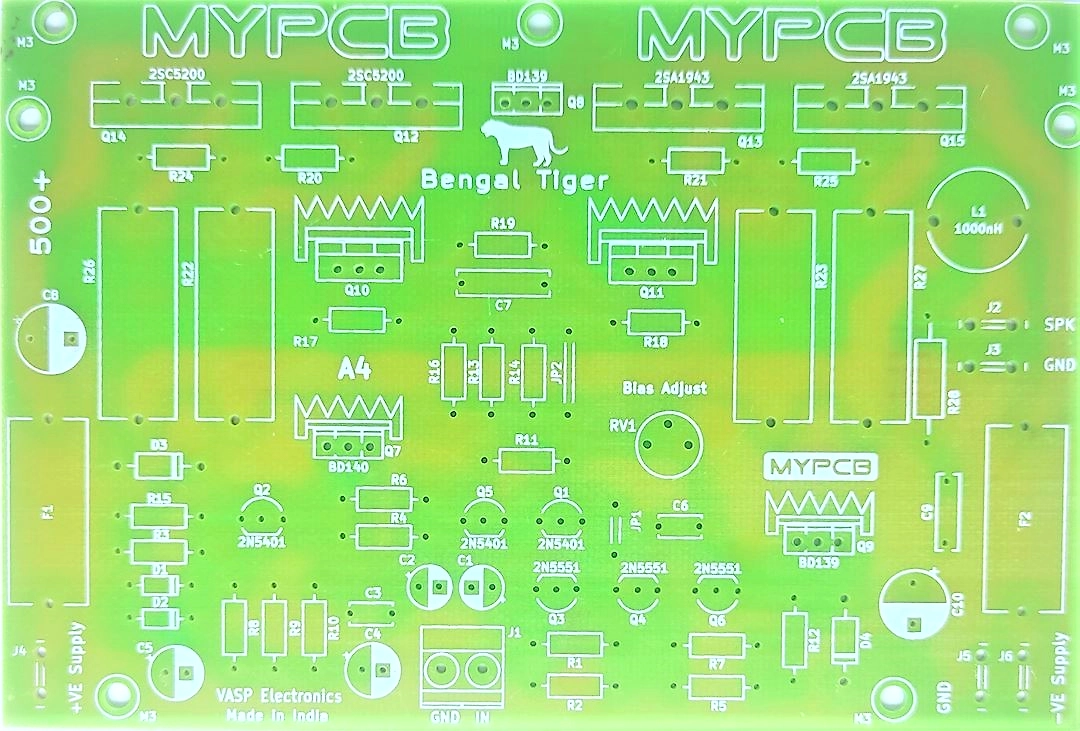
PCB Specification -
- Type of PCB - Single sided, Glass Epoxy FR-4 Grade A
- PCB size - 130 mm x 82 mm (5.1 inch x 3.2 inch ), pcb Thickness - 1.6 mm.
- Thickness of copper on PCB - 35 micrometer
PCB designed with thick copper tracks & large solder pads to facilitate straightforward placement and soldering of components.
Compatible / Replacement Part no. with Datasheet download links.*
Transistors
- Q10 - 2SC2073, 2SC4793, TIP41C, MJE15028-30-32
- Q11 - 2SA940, 2SA1837, TIP42C, MJE15029-31-33
* - Always use complementary NPN-PNP transistor pairs.
Installation:-
· Always use good quality Soldering Iron and Solder wire. After soldering components, check for solder overflow / dry / non-connections or shorted solder joints, else the amplifier will not work.
· Always use good quality heat sink paste and/or thermal pads between the components and heat sink.
· Securely Fix Biasing , Drivers and Power Transistors on suitable heat sink with insulators.
· Do not exceed recommended supply voltages.
· Never operate the Amplifier without a heat sink.
· If possible, try to connect the Ground Terminal of speakers to the power supply board.
· Before applying power - check for any short circuits between power supplies, input, output and ground.
· Before applying power - make sure the biasing potentiometer (RV1) is in center position.
· To Set biasing current - slowly adjust the Biasing Pot (RV1) without input signal. Test voltage across TP1 and TP2, idle Biasing current of 10 -15mA (4.4mV - 6mV ) will work fine in most conditions. Suggested Optimum Biasing current = 30 - 40mA ( 13.2mV - 17.6mV ).
· To set Gain - R2, R11 = 22K Gain = 26.8 dB (Normal Gain) for use with Pre amps and mixers.
R2, R11 = 33K Gain = 30.4 dB (High gain) for use with input from mobile phones / USB players.
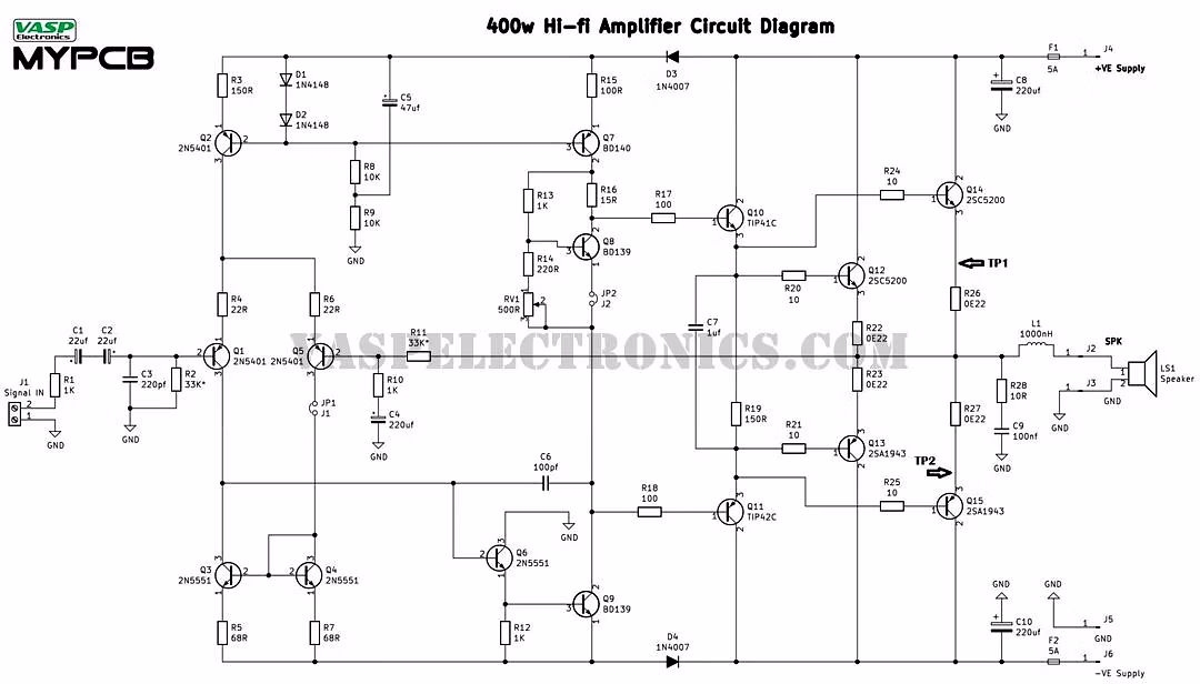 400w Hi-fi Amplifier Circuit Diagram