Buy PCB's Kits and Components for Audio Amplifiers Pre Amps BT boards Power supplies solar charge controllers Vu Meters & electronics parts at best price
- (+91) 9424930058
- mypcbinfo@gmail.com
- Amphead Electro Works, Aashish Complex, Ward No. 03 NH-46, Itarsi, Itarsi, Madhya Pradesh, India. 461111
© 2020 MYPCB. All Rights Reserved

Introduction
In making this simple but exceptionally well performing amplifier, we took inspiration from the original HITACHI lateral mosfet circuit from 1970's which was used in many famous sound systems and guitar amplifiers.
you can find the the original circuit HERE and an old British version HERE.
Very few components required, just one capacitor in signal path.
Experience uncolored sound of this simple circuit, you will love it.
New version of PCB having Space for Fitting Heatsinks easily.
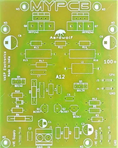
100w mosfet amplifier pcb
Features of 100 watt MOSFET Amplifier Board
- High output - 100 watt Dynamic output power.
- Low distortion - 0.07% Total Harmonic Distortion at 70 watt output using 8 ohms speakers and 1KHz sine wave input.
- Speaker usability - 4 & 8 ohms, 50 watt to 200 watt speakers can be used.
- Supply voltage - ±18 volts to ±35 volts DC supply working range.
- TO-220 Mosfet support - small farm factor mosfets like IRF540 IRF640 can be used.
- Standard components - All components used are available online or at your local electronics store.
- No SMD components used - Only through hole components used, making soldering and replacement hassle free.
- Cost effective - This amplifier can be made in a fraction of cost compared to similar amplifiers available in market.
Minimalist amplifier - Maximum performance
With this amp you can make -
- Subwoofer Amplifier - High power amplification of low frequency sound.
- Musical instrument amplifier - Frequency response 20 Hz to 50 KHz, you can amplify any instrument like Guitar, Keyboard, Banjo.
- Amplified speaker box - Compact size board that can be fitted inside the speaker enclosure.
- Stereo Amplifier - Listen to your favorite songs in clarity you never experienced before.
- Learning tool - Simple circuit to learn audio amplification basics.
Brief description of 100 watt mosfet amplifier circuit :-
Input Stage
Input stage works as a transconductance amplifier (voltage in - current out).
This stage consist of Long Tailed Pair (LTP) made of Q1 & Q2 working as differential amplifier.
Input signal received at the base of Q1 is amplified and sent to VAS from collector.
Negative feedback (NFB) received at the base of Q2 from output determines overall gain and balance of the amplifier. Current is supplied to the LTP by resistor R4.
In simple words input signal is amplified by the input pair Q1 & Q2 and sent to VAS for further amplification.
Voltage Amplification Stage (VAS)
As the name suggests, all the voltage gain of the amplifier is achieved in VA Stage.
Signal received from input stage at the base of Q5 is Voltage amplified and sent to the gate of mosfet Q7.
In simple words signal received from input stage is amplified by Q3 & sent to output stage.
Output Stage ( OPS )
This circuit has Class B output stage, so each half of the signal is amplified by each N-channel and P-channel mosfet.
Zobel Network - made of R15 & C6, provides protection against high frequency oscillations.
In simple words signal received from VAS is given to the output mosfets. Output mosfet conduct high current to drive the speakers load.
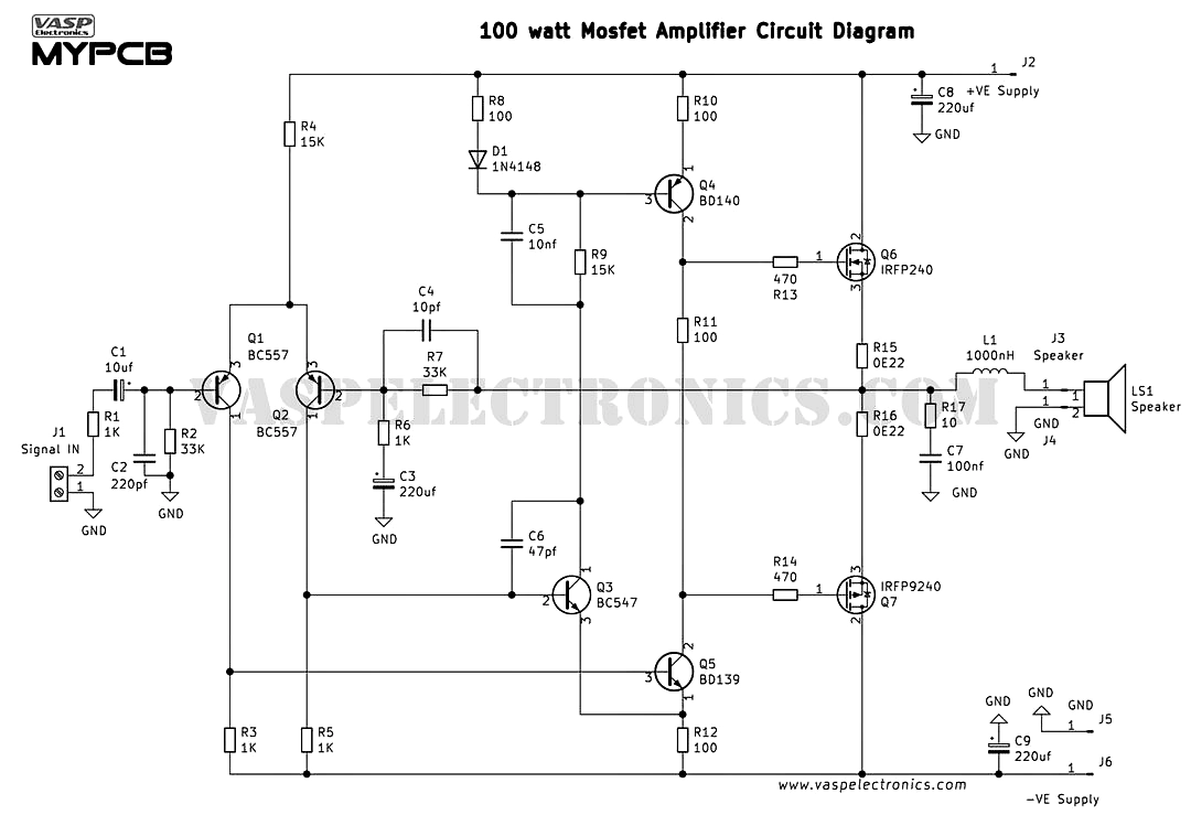 100w mosfet amplifier circuit diagram