Buy PCB's Kits and Components for Audio Amplifiers Pre Amps BT boards Power supplies solar charge controllers Vu Meters & electronics parts at best price
- (+91) 9424930058
- mypcbinfo@gmail.com
- Amphead Electro Works, Aashish Complex, Ward No. 03 NH-46, Itarsi, Itarsi, Madhya Pradesh, India. 461111
© 2020 MYPCB. All Rights Reserved

Introduction
Some of our customers wanted a simple amplifier which any one can make.
So we made a Basic amplifier board using minimum components.
It is easy to assemble and has decent performance,
Those who wish to learn Transistor amplifier basics can start with this Amp.
Professionals and Hobbyist will also find this amplifier useful for many applications.
New Version of PCB have space and Holes for Fitting Heat sinks Easily.
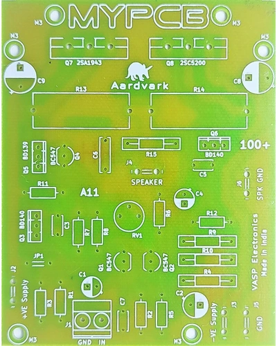
100w mono amplifier pcb
Features of 100 watt amplifier
- High Power - 100 watt Dynamic Output Power .
- Low distortion - 0.05% Total Harmonic Distortion at 60 watt output using 8 ohms speakers and 1KHz sine wave input.
- Speaker usability - 4 & 8 ohms, 50 watt to 200 watt speakers can be used.
- Supply voltage - ±18 volts to ±35 volts DC supply working range.
- Standard components - All components used are available online or at your local electronics store.
- No SMD components - Only through hole components used, making soldering and replacement hassle free.
- Cost effective - This amplifier can be made in a fraction of cost compared to similar amplifiers available in market.
Basic, Simple, Easy, Efficient Amplifier to Make -
- Subwoofer Amplifier - High power amplification of low frequency sound.
- Musical instrument amplifier - Frequency response 20 Hz to 50 KHz, you can amplify any instrument like Guitar, Keyboard, Banjo.
- Amplified speaker box - Compact size board that can be fitted inside the speaker enclosure.
- Stereo Amplifier - Listen to your favorite songs in clarity, you never experienced before.
- Learning tool - Simple circuit to learn audio amplification basics.
Brief Description of 100 watt amplifier circuit :-
Input Stage
Input stage works as a transconductance amplifier (voltage in - current out).
This stage consist of Long Tailed Pair (LTP) made of Q1 & Q2 working as differential amplifier.
Input signal received at the base of Q1 is amplified and sent to VAS from collector.
Negative feedback (NFB) received at the base of Q2 from output determines overall gain and balance of the amplifier. Current is supplied to the LTP by resistor R4.
In simple words input signal is amplified by the input pair Q1 & Q2 and sent to VAS for further amplification.
Voltage Amplification Stage (VAS)
As the name suggests, all the voltage gain of the amplifier is achieved in VA Stage.
Signal received from input stage at the base of Q3 is Voltage amplified and sent to the base of driver transistor Q5.
Current is supplied to VAS by resistor R9 & R10.
Biasing circuit is made of transistor Q4, which works as voltage divider. With preset RV1, base current of output transistors can be precisely adjusted.
Important to note that the biasing transistor Q4 & driver transistor Q5 can be tied together for better thermal tracking.
In simple words signal received from input stage is amplified by Q3 & sent to output stage.
Output Stage ( OPS )
This circuit has Class AB output stage, so each half of the signal is amplified by each NPN and PNP output transistors.
Driver Transistors Q5 & Q6 work as buffers to prevent excessive loading of VAS and also provide input to the output transistor Q7 and Q8 respectively.
Output Topology is Complementary Feedback pair which has improved linearity and better thermal tracking.
Zobel Network - made of R15 & C6, provides protection against high frequency oscillations.
In simple words signal received from VAS is given to the output transistors via driver transistors. Output transistors conduct high current to drive the speakers load.
Compatible / Replacement Part no. with Datasheet download links.*
Transistors
- Q1, Q2, Q4 - BC546-547-548-549-550
* - Always use complementary NPN-PNP pairs.
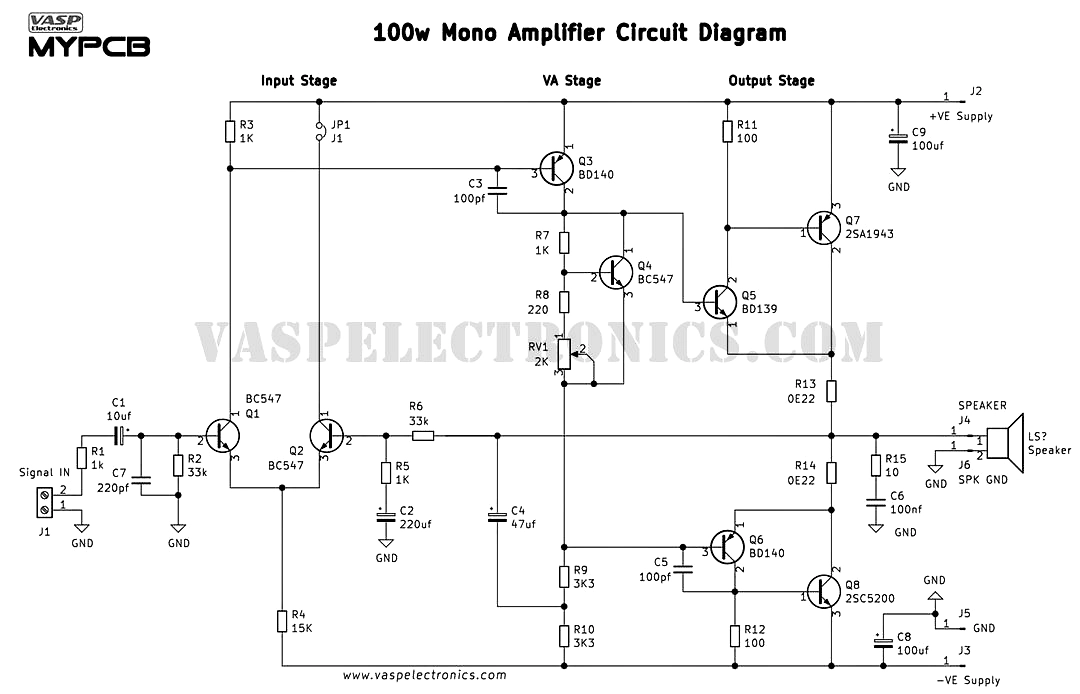 100 watt mono amplifier circuit diagram